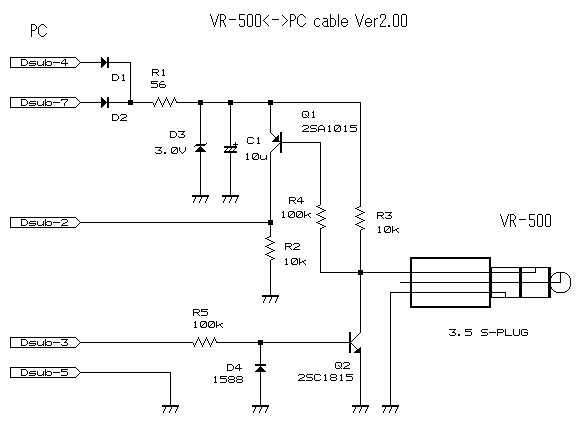
RIGHT STUFF, Inc.Right Stuff Wrong StuffVR-500(Ver3) I reconsidered the circuit.
The biggest change is using PNP transistor instead of NPN transistor that drive No.2 pin of RS-232C. Another change is the way to make 3.0V. I used both No.4 and No.7 pin for power source. Zener diode was not changed but R1 was reduced. R1 may be not necessary. But I left 56ohm. Because I want to keep the consumption of zener diode under 500mW even if very powerful 12V is impressed. Electrical Characteristics is not same between different brand zener diode at low current. Thus we need cut and try about R1 and Vz. If you feel this part is not cool, please use 3.0V regulator(low current consumption) or TL431 etc..
I used 4c cable. Because I had no choice but to use 4c. So I placed two diode in the D-sub shell.
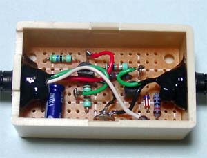
Inside of the box.
This time I wanted to check the wave form at some point. And delicate job is bother... Big box is acceptable for me.
Finally, I can edit the memory of my VR500. This cable and TK500 are very useful. Thank you ! "TK500".
|
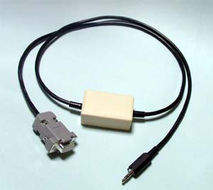 The circuit worked well on the bread board. I assembled the "PC I/F cable for VR500" using my junk parts.